
Process Flow
Indiana's advanced packaging facility handles back-end processing to bring High Bandwidth Memory (HBM) chips to market. Wafers with pre-formed vertical electrical connections undergo a series of advanced processing steps to produce fully-integrated HBM products.
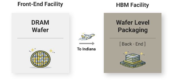
HBM Process Flow
High Bandwidth Memory (HBM) is a high-performance memory chip built for speed. As modern computing demands greater processing power, HBM has become a go-to solution. These chips are made using Through-Silicon Via (TSV) technology formed at the wafer level during the front-end process. Multiple chips are then vertically stacked - like a skyscraper - through the advanced back-end packaging processes. This stacking allows data to travel faster, uses less power and keeps the overall size compact.
Front Bump Formation
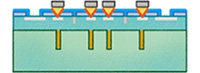
HBM, which is built through chip stacking, requires a structure that enables electrical connections between individual chips. This structure is known as a bump. The process begins with forming bumps on the front of a wafer, and these bumps are created through an electroplating process.
Wafer Solder Reflow

To facilitate chip-to-chip bonding, the top surface of the formed bumps is made of solder. A reflow process is then performed to melt the solder and re-form it into a spherical shape. This process creates a physically stable ball structure, reduces surface area, and improves solder wettability for reliable interconnection.
Temporary Carrier Bonding
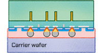
Once the front bumps are properly formed, a process is carried out to attach a carrier wafer to protect and facilitate handling of the front side during back bump formation. In this process, an adhesive is applied, and the carrier wafer is temporarily bonded using heat and pressure.
TSV Exposure & Back Passivation
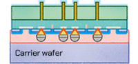
After the carrier wafer is bonded, a back processing step is performed to expose the top of the vertical interconnect access (via) on the backside. The silicon surface of the wafer back is etched, and a passivation layer is subsequently formed to prevent copper diffusion.
Passivation CMP & TSV Copper Exposure
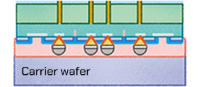
After the pre-processing steps are completed, a CMP (Chemical Mechanical Polishing) process is carried out to expose the vias through mechanical abrasion. Once the CMP process is completed, the vias are exposed, enabling the back bump formation process on the wafer.
Back Bump Formation
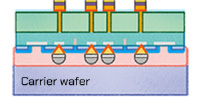
Back bumps are formed using an electroplating process, similar to the process used on the front side.
Carrier Wafer Debonding & Thin Wafer Mounting on Tape
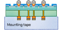
Once the formation of the back bumps is completed, the backside of the wafer is attached to a mount tape, and the previously bonded carrier wafer is removed. Afterward, several subsequent processes are performed to separate the wafer into individual chips.
Chip Stacking & PKG Assembly With Overmold
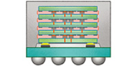
After the wafer is separated into individual chips, they are stacked on top of the base wafer, which forms the bottom foundation of the HBM. The stacked wafers are then molded using an epoxy mold compound (EMC), and the product after this molding process is referred to as mKGSD (Molded Known Good Stacked Die). Finally, the mKGSD is diced to complete the HBM chip as we know it.
For information regarding emissions, please refer to the FAQ section on our website and WLmoves website (WLmoves.com)